- 您现在的位置:买卖IC网 > Sheet目录514 > SIHG20N50C-E3 (Vishay Siliconix)MOSFET N-CH 500V 20A TO247
SiHG20N50C
Vishay Siliconix
1
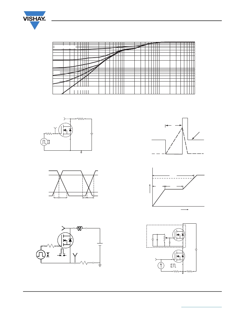
Duty Cycle = 0.5
0.2
0.1
0.1
0.05
0.02
Single Pulse
0.01
10 -4
10 -3
10 -2
0.1
1
Pulse Time (s)
Fig. 10 - Normalized Thermal Transient Impedance, Junction-to-Case (TO-247)
V DS
R D
V DS
R g
V GS
D.U.T.
+
- V DD
t p
V DD
10 V
V DS
Pulse width ≤ 1 μs
Duty factor ≤ 0.1 %
I AS
Fig. 11a - Switching Time Test Circuit
Fig. 12b - Unclamped Inductive Waveforms
V DS
90 %
10 %
V GS
10 V
V G
Q GS
Q G
Q GD
t d(on)
t r
t d(off) t f
Fig. 11b - Switching Time Waveforms
L
Charge
Fig. 13a - Basic Gate Charge Waveform
Current regulator
Vary t p to obtain
required I AS
V DS
Same type as D.U.T.
50 k Ω
R g
D.U.T
I AS
+
-
V DD
12 V
0.2 μF
0.3 μF
D.U.T.
+
-
V DS
10 V
t p
0.01 Ω
V GS
3 mA
Fig. 12a - Unclamped Inductive Test Circuit
I G
I D
Current sampling resistors
Fig. 13b - Gate Charge Test Circuit
Document Number: 91382
S11-0440-Rev. C, 14-Mar-11
www.vishay.com
5
This datasheet is subject to change without notice.
THE PRODUCT DESCRIBED HEREIN AND THIS DATASHEET ARE SUBJECT TO SPECIFIC DISCLAIMERS, SET FORTH AT www.vishay.com/doc?91000
发布紧急采购,3分钟左右您将得到回复。
相关PDF资料
SIHG24N65E-E3
MOSFET N-CH 650V 24A TO247AC
SIHP12N60E-E3
MOSFET N-CH 600V 12A TO220AB
SIHP30N60E-E3
MOSFET N-CH 600V 29A TO220AB
SIHP5N50D-E3
MOSFET N-CH 500V 5.3A TO220AB
SIHP6N40D-E3
MOSFET N-CH 400V 6A TO-220AB
SIHP7N60E-GE3
MOSFET N CH 600V 7A TO-220AB
SIHU3N50D-E3
MOSFET N-CH 500V 3A TO251 IPAK
SIHU5N50D-E3
MOSFET N-CH 500V 5.3A TO251 IPAK
相关代理商/技术参数
SIHG22N50D-E3
功能描述:MOSFET 500V 22A 312W 230mOhm @ 10V
RoHS:否 制造商:STMicroelectronics 晶体管极性:N-Channel 汲极/源极击穿电压:650 V 闸/源击穿电压:25 V 漏极连续电流:130 A 电阻汲极/源极 RDS(导通):0.014 Ohms 配置:Single 最大工作温度: 安装风格:Through Hole 封装 / 箱体:Max247 封装:Tube
SIHG22N50D-GE3
功能描述:MOSFET 500V 230mOhm@10V 22A N-Ch D-SRS
RoHS:否 制造商:STMicroelectronics 晶体管极性:N-Channel 汲极/源极击穿电压:650 V 闸/源击穿电压:25 V 漏极连续电流:130 A 电阻汲极/源极 RDS(导通):0.014 Ohms 配置:Single 最大工作温度: 安装风格:Through Hole 封装 / 箱体:Max247 封装:Tube
SIHG22N60E
制造商:VISHAY 制造商全称:Vishay Siliconix 功能描述:E Series Power MOSFET
SIHG22N60E_13
制造商:VISHAY 制造商全称:Vishay Siliconix 功能描述:E Series Power MOSFET
SiHG22N60E-E3
功能描述:MOSFET 600V 180mOhm@10V 21A N-Ch E-SRS
RoHS:否 制造商:STMicroelectronics 晶体管极性:N-Channel 汲极/源极击穿电压:650 V 闸/源击穿电压:25 V 漏极连续电流:130 A 电阻汲极/源极 RDS(导通):0.014 Ohms 配置:Single 最大工作温度: 安装风格:Through Hole 封装 / 箱体:Max247 封装:Tube
SIHG22N60E-GE3
功能描述:MOSFET 600V 180mOhm@10V 21A N-Ch E-SRS
RoHS:否 制造商:STMicroelectronics 晶体管极性:N-Channel 汲极/源极击穿电压:650 V 闸/源击穿电压:25 V 漏极连续电流:130 A 电阻汲极/源极 RDS(导通):0.014 Ohms 配置:Single 最大工作温度: 安装风格:Through Hole 封装 / 箱体:Max247 封装:Tube
SIHG22N60E-GE3
制造商:Vishay Siliconix 功能描述:MOSFET N CH 600V 21A TO-247AC-3
SiHG22N60S
制造商:Vishay Semiconductors 功能描述:
